Class D
Audio Amplifier Design
Example design: TDA7498
High
performance on a (power) budget
author: Trevor Marshall

 |
Class D
|
 |
Discussion
/ Questions
on the DIYaudio
Class-D forum, please
Why another tutorial on Switched Power Amp design?
A couple of years ago
I decided I would (eventually) need to replace my decades-old Nakamichi
stereo with something more suited to a mobile lifestyle. It was
immediately pretty obvious that the Class-D and E switching amplifiers
I had
researched in the '70s were experiencing a renaissance. Tripath had
come and gone, but its excellent chipsets remained available from
China. ST had a few nice chips, as did National Semi, Texas
Instruments and IR.
I quickly found that the science developed in the '70s, a deep understanding of the differences between switched amplifiers and linear amplifiers, seems to have been forgotten. Sure, the chipsets are really excellent, but the component selection in the application designs seemed to be pretty woeful. Since most of the new chips have a feedback loop which doesn't include the output filter circuit, poorly designed filter networks were limiting the performance of most of the amplifier modules commonly available.
I have been playing with several chipsets, those which I think have the most potential for value-HiFi, and I am going to use the ST TDA7498 chip to illustrate how not to design a quality audio amplifier, and how inexpensive it can be to design a good one..
ST don't supply
boards for the TDA7498, so I bought some assembled PCBs on
Ebay from
Sure Electronics (for the princely sum of $22)(#AA-AB32165).
Although
they were advertised as TDA7492
boards, several arrived with TDA7498 on
them, but the last one came with a TDA7492. So haggle with the seller a
little, if
you need to operate above a 24V supply rail. I was able to change the
chips, but I needed my special surface mount rework tools. SURE
assembles these PCBs identically for both CPUs, except that the fan
power supply components are added for the TDA7498 version.
I initially had resolved not to use any Chinese-supplied CPU on the
tutorial boards, but in retrospect, the TDA7498 on the SURE boards
turned out to be
effectively identical with the full spec TDA7498TR devices I purchased
from
Mouser.
It didn't take much testing to discover the first problem with the SURE assemblies. A sweep of distortion vs frequency (8 ohm load) came nowhere near the data sheet specification.
 |
(Distortion of -40dB
corresponds to 1%, -60dB to 0.1%, and so on) So the measured level of 2-3% above 5KHz should be closer to 0.2%, if the data sheet is accurate  |
The distortion at higher frequencies was ten times what the data sheet predicted, peaking at an unacceptable 3% or so... The big steps at the higher frequencies on my graph occur as the 3rd harmonic goes outside the audio range and eventually as the 2nd harmonic also become too high to detect. The data sheet graph shows the same phenomenon, but it is masked by excessive smoothing of their curve data...
To demonstrate how important it is to carefully design an audio system, the change of just one component on the board (per channel) largely corrects this problem, bringing performance much closer to what I had expected to be buying:
This transformation to a maximum HF distortion level of about 0.3% was achieved by replacing the 1uF X7R ceramic output capacitor (surface mount C14,C18) with an MKS polyester capacitor of the same value. Click here for a Maxim application note describing the problem with using X7R ceramic capacitors in high current circuitry.
Referring to a copy of the schematic
for the TDA7498
SURE circuit board, it is interesting to note that SURE using the
other two ceramic capacitors in the output filter (C15,C16,C19,C20) has
had a much smaller
impact on circuit distortion (as we will see
in a later section of this tutorial).
You might choose to replace the two input coupling capacitors (C21,C22) with 0.47uF-1uF MKS to deal with that extra low frequency distortion (discussed in the Maxim application note). And while we are at it, why don't we replace the other parts that SURE left off their assemblies?
TP5 and TP6 are
convenient places to put the 1000pf HF
bypass capacitors from chip pins 22 and 32 to ground (scrape away a
little of the green solder mask from ground plane for the ground
connection). You might want to
decrease the clock frequency resistor R5 to 30K (from 33K), and we must
put in the snubber circuits which ST recommend at R6,R7,C13 and C17.
Please use the data sheet values of 330pf and 22 ohms. Ignore (for now)
those yellow caps in the output filters on the left of the board...
|
When removing the heatsink, remember not to lose the four white spacers between the heatsink and the PCB. |
|
So at this point we have a circuit board which follows the data sheet application-circuit fairly closely. The next thing to consider is the output filter. Its job is to average out the PWM current pulses from the TDA7498 output transistors, smoothing them into a signal which is flat, and low distortion, across the audio spectrum. But just as important, and something that designers seem to have forgotten these days, is (1) that filter should not cause the amplifier feedback loop to go unstable, and (2) that we don't want the filter to create huge currents when the amp is driving a real HiFi speaker, rather than a purely resistive dummy-load. Out-of-the-box,
the output filter design used by SURE is unstable. I guess somebody
wanted to save a few cents by omitting the filter damping resistors.
Sigh... Here
is a sinewave output on which you can clearly see there are quite large
transient spikes being generated as the output circuitry loses control
of the high currents circulating in the (undamped) filter circuit. |
|
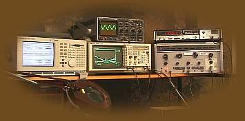
Here is the output voltage seen in a typical Class-D amplifier with a slightly underdamped output filter. You can see the PWM 3usec signal (330KHz) superimposed on the lower frequency square-wave, and you can see the overshoot (at about 25KHz) which has resulted from the underdamped filter, resonant in the mid-20s KHz. This is, of course, a storage scope trace of a single sweep. On an analog 'scope you would see a continuous blur, whilst the individual 330KHz sinusoids can be distinguished on the HP 'scope. Designing an
output filter is always a compromise between critical damping,
necessary for a flat frequency response and minimal overshoot, and the
variety of complex impedances which are connected at the output of an
audio amplifier ('complex' in the sense of being inductive and
capacitive, as well as resistive). |
It is important to
talk a little bit about filter topology. You will find filter design
criteria, such as
this article from ST Engineers
which gives rigorous-looking formulae for output filter design. Sadly,
there is no set
of formulae which can help you cope with feeding a high quality wide
range speaker, which, eg,
looks like a 6.1
ohm resistance in series with a 0.64mh inductance, or 3.6ohm
in
series with 0.03mh. These are the speakers I selected for my new
"ground effect omnidirectional" loudspeaker system, a SEAS L16RN
and a Peerless Tymphany 830983 -- bi-amped using a MiniDSP
crossover, with two of these SURE
boards
being fed from a 36V power brick. The SEAS woofer is essentially an
open circuit at the filter resonant frequency
(in the mid '20s KHz), while the Peerless widerange is really not much
easier to drive, even though its audio response is pretty good right up
to supersonic frequencies.
|
In 1978 I had to
use a
circuit simulator called SPICE to simulate what
would happen to my designs when a reactive load was connected, and in
2011 SPICE is still the best choice. Luckily, during the intervening
years,
National
Instruments has
thrown a wonderful GUI around it ('MultiSIM'). The first issue to be solved is the optimum filter circuit topology to be used. Wider and Zhao described several in their article, and discussed the tradeoffs. But they did not canvas the issue of reactive loads (speakers) and feeding these highly reactive loads forced me to develop yet another topology (at left). The primary
practical design issues to be solved are the choice of inductor and the
power rating of the damping resistor. Polyester acapcitors are assumed,
and their quality is pretty good these days. I wish the same could be
said for the inductors, I have a graveyard of inductors from many
manufacturers and of many specifications, trying to find some which
would perform linearly, without excessive temperature rise at the
relatively high (400KHz) voltages involved. I tried all the inductor
brands Mouser had in stock, brought inductors in from Hong Kong, and
even took inductors off other Class-D amplifiers. Not one inductor was
perfect. The ICE 1D14A and 1D17A series
were the best overall
performers I found, but I selected Bourns
SRF1280-150M for my SURE
boards as they soldered into the same footprint as the original
inductors used by SURE, and had adequate current handling for the
TDA7498 operating on 32V DC. |
The second major tradeoff in inductor design is its value. Should one use 10uH, 15uH, 22uH or 33uH? SURE chose 33uH, presumably because the higher inductances don't heat up so much from the quiescent core-magnetization flux. But to drive 4 ohms I needed 10uH or 15uH, while compatibility with 8 ohm loads pushed us towards the 15uH choice. So 15uH it was. And the SRF1280-150M was the only small inductor which stayed reasonably cool and linear when the TDA7498 was on the 32 volt supply. I think it has a higher quality core material, as it is intended for use in transformers, not just filter inductors.
The polyester film output capacitors are soldered to the pads conveniently offered by the (unused) banana-plug pads on the left hand end of the board (see photo above). The ground connection for the two 330nf/63V capacitors is made by scraping some of the green solder-resist mask off the area between the banana-plug holes, where there are vias through to the ground plane. The 220nF/63V and its 22 ohm resistor are soldered "dead bug style" onto the board, as seen in the photo. I have used only a 1 watt damping resistor, as I will not have a significant level of high-frequencies going though these amps. The SEAS woofer crossover is at 200Hz, while the Peerless widerange 'tweeters' become deafening at just a few watts... But if you are going to be stressing these amps with lots of treble above 10KHz, I suggest using a 2 watt (or 5 watt) 22 ohm metal-film resistor.
|
For light
entertainment, |
|
By comparison, at left is the frequency response of the SURE board, fully modified as I have described, when connected to an 8 ohm resistive load. The 4 ohm response is to the right. |
|
The modded board has very low distortion, significantly less than 0.1% THD into 8 ohms, and only a little higher into a 4 ohm load. My ability to measure distortions in the -70dB range is limited by random noise pulses in my workbench and power supplies, and by difficulty getting the FFT-based software to reliably lock onto signals which are only just above the -120dB noise floor of my computer's 24-bit sound input card. Here are the sweeps of distortion vs frequency at 4V RMS output voltage (a couple of watts). The 8 ohm curve is on the left, the 4 ohm on the right. |
|
Distortion vs
output Power for the modded TDA7498 board. The 8 ohm curve is on the
left, the 4 ohm on the
right. Note that I had to manually stop the sweep with the 4 ohm load
before reaching clipping,
as the TDA7498's internal current limiting kicked in at levels
above 80W with a 32V supply. Ulrich
M�ller's wonderful "Audio tester"
software allows multiple curves to be plotted for this test mode, one
for each of the second, third, fourth and fifth harmonics, and I have
done this, so as to show that the odd harmonics rise rapidly at the
clipping threshold, as expected. |
It is worth exploring why the TDA7498's output current protection kicks in (with a 32V supply) when one tries to drive 100W into a 4 ohm load. The raw arithmetic is pretty simple -- 29V p-p output signal in bridge configuration yields 58V p-p into the load. Imax = Vmax/R, or 7.25 amps peak. This is just above the maximum current spec of a TDA7498, and the chip in my two test boards clearly did not allow any margin for error. When protection kicks in, it is latched until the standby circuitry time constant has discharged (a few tens of milliseconds). You can connect a LED-driving transistor to TP7 (near the input caps) if you want a visual indication when the protection circuitry kicks in.
|
What is less obvious that the current protection may also kick in with no speaker attached at all, due to circulating currents in the output filter. The SPICE/Multisim bode plots showing this artifact is at right. Using the complex "8 ohm" SEAS L16RN woofer impedance as a load, the current from the TDA7498's outputs at low frequencies is shown on the bottom plot (100Hz-300KHz, 10 amps fullscale) as about 6 amps throughout the woofer's frequency range. But the current peaks to about 7 amps at 61KHz, due to filter currents. In the absence of an optimum damping resistor, filter currents can go well above 10 amps if high frequencies are inadvertently allowed through by preamp circuitry... In my case, the MiniDSP crossover makes sure this will not happen. The bode plots also show the predicted frequency response (middle plot, 10 dB/division), while the top plot shows the voltage across the damping resistor (full scale=34 volts), with the 1 watt dissipation frequency marked by the cursor. |
|
You can download the MultiSim simulation file which produced those Bode plots by clicking here. It will run with
the MultiSim evaluation version , which you can download and
install from NI.com, or with any of the commercial versions of MultiSim, including
the student version. I have placed 0.01 ohm resistors in series with
the inductors to allow me to plot the inductor (and FET switch)
currents. There are three Bode plotting instruments, XBP1 for the
inductor current, XBP2 for the output voltage vs frequency response,
and XBP3 to show the voltage across the damping resistance, and hence
allow its power dissipation to be calculated. A compromise has to be
struck between power dissipated in this resistor at high frequencies,
and the damping applied at the filter resonance. In this case, I
decided to ensure that the peak current was just within the
capabilities of the FET switches in a good TDA7498 (7 amps typ.). |
Summary.
This filter I designed
for the TDA7498 will work with any
of the >50W bridged switching amplifiers, as long as you pay
attention to capacitor voltages and inductor current. You can expect
similar frequency response and
stability with other bridged chipsets. Remember that the peak inductor
current, and therefore the chip output transistor current, can
reach 7 amps with this filter design, and much more if a properly
designed filter is not used. It is best to make sure that
any amplifier you select has effective over-current-protection on its
output devices.
I hope you found this
discussion interesting, please ask any technical questions on the
DIYaudio
forums.
Copyright (C) 2012 Trevor G Marshall, All Rights Reserved